itsallgoodjames
Hazard to Others
  
Posts: 276
Registered: 31-8-2020
Location: America Lite
Member Is Offline
|
|
Formation of a thin layer layer of SiO2 on the surface of an Si wafer coated in Ag without using sputtering
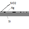
So I need a way to create a thin (a few hundred nm thick) non-conductive oxide layer that works on silver and silicon. Growing an oxide layer
thermally won't work, as it needs to coat both the Si and Ag areas with the same height of oxide, as shown (image not remotely to scale):

So far what I'm thinking is spin coating the wafer with SiCl4, then spinning on a layer of water to turn it into SiO2. Does that sound like it would
work? My main concern is that the moisture in the air will react with it while it's being spun on, causing it to look more like this

Is that a problem I need to worry about? Will this even work at all? Is there any other ways to make a thin layer of a non-conductive oxide? Is
there an oxide that would work better than SiO2?
Thanks
Nuclear physics is neat. It's a shame it's so regulated...
Now that I think about it, that's probably a good thing. Still annoying though.
|
|
|
njl
National Hazard
   
Posts: 609
Registered: 26-11-2019
Location: under the sycamore tree
Member Is Offline
Mood: ambivalent
|
|
I really doubt that would work, You'd likely end up with a bunch of sand and a ruined wafer. What is the context here? Do you want a homogeneous layer
like a sheet of glass or a heterogeneous layer like concrete or sintered metal?
Reflux condenser?? I barely know her!
|
|
|
itsallgoodjames
Hazard to Others
  
Posts: 276
Registered: 31-8-2020
Location: America Lite
Member Is Offline
|
|
I want a homogeneous layer, similar to what you would get if you were to sputter it on. I don't have (and can't afford) a sputtering setup
Nuclear physics is neat. It's a shame it's so regulated...
Now that I think about it, that's probably a good thing. Still annoying though.
|
|
|